-
Viewpoint on 'IONS'
Viewpoint on 'Scientific Literacy'
- Proudly sponsored by
-


-
Sailing through the Waves of Light
The difference in the interaction between an atom and light can be as wide as that between a pleasant, relaxing canoe ride, and a whitewater rafting experience. It is now possible to switch back and forth between the two, ultraquickly, at the touch of a laser pulse.
-
Why We Need Young Scientists to Interact with Companies

Young researchers play a significant role in the flourishing of innovation by embracing the challenges at the boundaries of academic and industrial R&D.
by Iain Ross -
Light from the Darkest Planet

The composition of exoplanets can be inferred from their reflected light. But, what if a planet is far darker than we had ever thought possible?
Volume 7 Story 1 - 5/10/2009
Plasmon Harvesting:
What cannot be seen can often be felt, even in the case of physics. Invisible electromagnetic oscillations, known as surface plasmons, trapped inside a nanowire can now be detected by converting them into an electrical current.
 Scientists have always been seduced by the challenge of detecting the invisible: they know that this has potentially revolutionary implications. In 1897, when J. J. Thomson detected electrons, he was taking a far-reaching step forward in the understanding of atoms. Now a team of scientists led by Hongkun Park from Harvard University, USA, and from Pohang University of Science and Technology, Korea, has devised a new method to detect small electromagnetic oscillations, also known as surface plasmons, which propagate along a nanowire. In a not-so-distant future, this might lead to plasmonic circuits that can be directly integrated with their electronic counterpart.
Have you ever been part of a human wave in a large crowd at a football or baseball game? This is precisely what happens to the free electrons on the surface of a thin metal when they are hit by light of the right color. Some electrons start oscillating and these oscillations are passed on to the neighboring electrons, thus forming a surface wave — a surface plasmon, that is [1]. Surface plasmons can propagate long distances along thin metallic structures, such as nanowires, provided they do not encounter any defects in the structure.
Controlling surface plasmons and guiding them through a specific path can lead to interesting science, for example to designing the optical equivalent to electronic circuits and to focusing light beyond the diffraction limit. Unfortunately, surface plasmons live trapped right underneath the metal surface, where it is not possible to detect them directly. The usual approach is to convert them into light, which can then be easily observed. The work of Hongkun Park and colleagues demonstrates a new way of detecting surface plasmons by converting them into an electrical current.
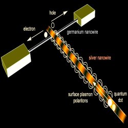
Just like a photodetector can convert photons into electricity, the new device can convert plasmons into electricity. It consists of two nanowires, one of silver and the other of germanium, crossing each other. The germanium nanowire, with two metal pads as contacts at its end, acts as a field-effect transistor. Surface plasmons are excited on the silver nanowire using a focused light. After propagating along the silver nanowire, the surface plasmons get coupled to the germanium nanowire at the junction. This coupling is achieved through a near-field interaction, similar to what happens when two wires carrying electric current are crossed together. Finally, the germanium nanowire transforms the plasmons into an electrical current. Hongkun Park explains the working mechanism of the device, "surface plasmons impinging on the Ag-Ge [silver-germanium] junction generate electron-hole pairs in the Ge [germanium] nanowire. These electron-hole pairs are then separated by the built-in potential at the junction created by the charge transfer between Ag [silver] and Ge [germanium], which are then detected as an electrical signal."
Electrical detection of plasmons had previously been shown on localized plasmons [2]. However, as the name itself indicates, such plasmons are localized on metallic nanoparticles and it is not possible to build photonic circuits out of them. This is now possible by using surface plasmons propagating that propagate along nanowires. For example, using this device it is possible to detect the photons emitted by a single photon source, such as a quantum dot, a nanometer-sized semiconductor particle that emits light upon proper excitation. Hongkun Park and colleagues have demonstrated that the photons emitted by a single quantum dot can be transformed into plasmons that propagate in the nanowire and that can eventually be detected as an electrical current.
One potential outcome of this research would be to replace electronic circuits with plasmonic ones. This, for example, would make for faster and cheaper optical communication. "SP [surface plasmon] circuits can, potentially, be faster than their electronic counterparts. Moreover, these SP circuits, unlike their electronic counterparts, can be used in many applications," comments Hongkun Park. He also envisions the possibility of directly imaging the surface plasmons simply by raster scanning the "plasmon detector" over the structure and collecting the current at each position.
The new technique brings us a step closer to plasmonic circuitry, even though much work remains to be done. Leo Kouwenhoven at the Delft University in the Netherlands says, "In general this is a new direction where optics and electronics are combined. This is extrememely important if new interfaces between the two are to be developed. However, the specific detection mechanism of the nanowire is not well controlled, so in the future this needs to be improved." The work by Park and colleagues is a big leap towards a plasmonic circuitry bridging the optical and electronic counterparts with great efficiency. In the coming future, photons, electrons, and plasmons all together will pass on information at speeds that are now still inconceivable.
[1] H. Raether, Surface Plasmons on Smooth and Rough Surfaces and on Gratings, Vol. 111 of Springer Tracts in Modern Physics (Springer-Verlag, Berlin, 1988).
[2] I. De Vlaminck, P. Van Dorpe, L. Lagae, and G. Borghs, Local Electrical Detection of Single Nanoparticle Plasmon Resonance, Nanoletters 7, 703-706 (2007).

Plasmon Harvesting:
A Route to Plasmonic Circuitry
What cannot be seen can often be felt, even in the case of physics. Invisible electromagnetic oscillations, known as surface plasmons, trapped inside a nanowire can now be detected by converting them into an electrical current.Detecting surface plasmons as electrons. Schematic of the device that converts surface plasmons into an electric current. It consists of a silver nanowire along which the surface plasmons propagate, and a crossing germanium nanowire, that converts the surface plasmons to electron-hole pairs. A quantum dot can be used to launch the surface plasmons along the nanowire. Figure courtesy: Abram L. Falk.
Have you ever been part of a human wave in a large crowd at a football or baseball game? This is precisely what happens to the free electrons on the surface of a thin metal when they are hit by light of the right color. Some electrons start oscillating and these oscillations are passed on to the neighboring electrons, thus forming a surface wave — a surface plasmon, that is [1]. Surface plasmons can propagate long distances along thin metallic structures, such as nanowires, provided they do not encounter any defects in the structure.
Controlling surface plasmons and guiding them through a specific path can lead to interesting science, for example to designing the optical equivalent to electronic circuits and to focusing light beyond the diffraction limit. Unfortunately, surface plasmons live trapped right underneath the metal surface, where it is not possible to detect them directly. The usual approach is to convert them into light, which can then be easily observed. The work of Hongkun Park and colleagues demonstrates a new way of detecting surface plasmons by converting them into an electrical current.
Just like a photodetector can convert photons into electricity, the new device can convert plasmons into electricity. It consists of two nanowires, one of silver and the other of germanium, crossing each other. The germanium nanowire, with two metal pads as contacts at its end, acts as a field-effect transistor. Surface plasmons are excited on the silver nanowire using a focused light. After propagating along the silver nanowire, the surface plasmons get coupled to the germanium nanowire at the junction. This coupling is achieved through a near-field interaction, similar to what happens when two wires carrying electric current are crossed together. Finally, the germanium nanowire transforms the plasmons into an electrical current. Hongkun Park explains the working mechanism of the device, "surface plasmons impinging on the Ag-Ge [silver-germanium] junction generate electron-hole pairs in the Ge [germanium] nanowire. These electron-hole pairs are then separated by the built-in potential at the junction created by the charge transfer between Ag [silver] and Ge [germanium], which are then detected as an electrical signal."
Electrical detection of plasmons had previously been shown on localized plasmons [2]. However, as the name itself indicates, such plasmons are localized on metallic nanoparticles and it is not possible to build photonic circuits out of them. This is now possible by using surface plasmons propagating that propagate along nanowires. For example, using this device it is possible to detect the photons emitted by a single photon source, such as a quantum dot, a nanometer-sized semiconductor particle that emits light upon proper excitation. Hongkun Park and colleagues have demonstrated that the photons emitted by a single quantum dot can be transformed into plasmons that propagate in the nanowire and that can eventually be detected as an electrical current.
One potential outcome of this research would be to replace electronic circuits with plasmonic ones. This, for example, would make for faster and cheaper optical communication. "SP [surface plasmon] circuits can, potentially, be faster than their electronic counterparts. Moreover, these SP circuits, unlike their electronic counterparts, can be used in many applications," comments Hongkun Park. He also envisions the possibility of directly imaging the surface plasmons simply by raster scanning the "plasmon detector" over the structure and collecting the current at each position.
The new technique brings us a step closer to plasmonic circuitry, even though much work remains to be done. Leo Kouwenhoven at the Delft University in the Netherlands says, "In general this is a new direction where optics and electronics are combined. This is extrememely important if new interfaces between the two are to be developed. However, the specific detection mechanism of the nanowire is not well controlled, so in the future this needs to be improved." The work by Park and colleagues is a big leap towards a plasmonic circuitry bridging the optical and electronic counterparts with great efficiency. In the coming future, photons, electrons, and plasmons all together will pass on information at speeds that are now still inconceivable.
[1] H. Raether, Surface Plasmons on Smooth and Rough Surfaces and on Gratings, Vol. 111 of Springer Tracts in Modern Physics (Springer-Verlag, Berlin, 1988).
[2] I. De Vlaminck, P. Van Dorpe, L. Lagae, and G. Borghs, Local Electrical Detection of Single Nanoparticle Plasmon Resonance, Nanoletters 7, 703-706 (2007).
Sudhir Cherukulappurath
2009 © Optics & Photonics Focus
SC is a research fellow at ICFO - The Institute of Photonic Sciences (Barcelona, Spain).
Abram L. Falk, Frank H. L. Koppens, Chun L. Yu, Kibum Kang, Nathalie de Leon Snapp, Alexey V. Akimov, Moon-Ho Jo, Mikhail D. Lukin, and Hongkun Park, Near-field electrical detection of optical plasmons and single-plasmon sources, Nature Physics (2009) 5, 475-479 (link).