-
Viewpoint on 'IONS'
Viewpoint on 'Scientific Literacy'
- Proudly sponsored by
-


Extreme Ultraviolet Lithography: Towards the Next Generation of Integrated Circuits
Optics & Photonics Focus
Volume 7 Story 4 - 4/11/2009
Optics & Photonics Focus
Volume 7 Story 4 - 4/11/2009
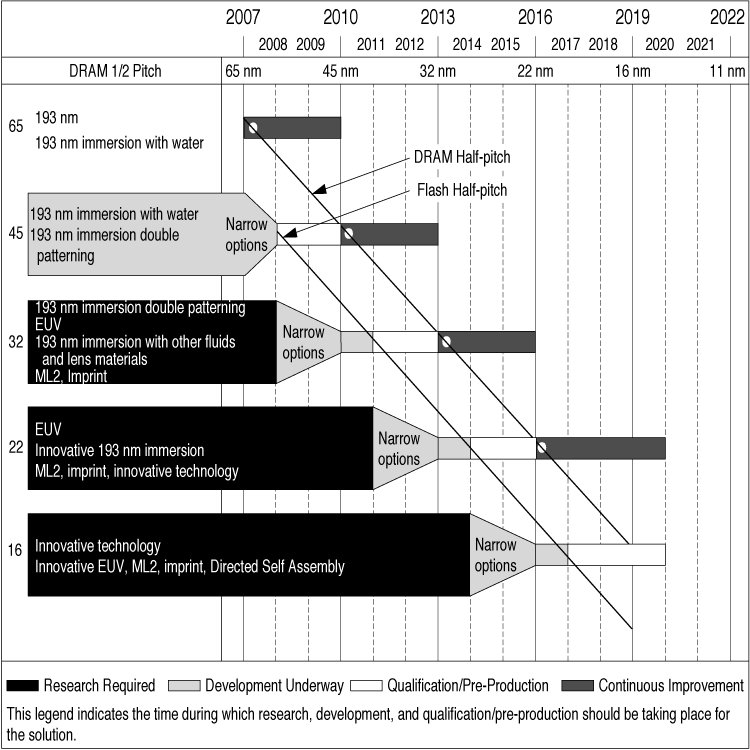
2007 ITRS lithography roadmap for semiconductors
At the moment, it is predicted that EUVL will have some pilot-scale applications at the 32 nm technology node or will be used in full production for the 22 nm half-pitch technology node. High volume manufacturing (HVM) pre-production (beta) exposure aligners will be delivered to multiple end-users starting in 2010.
Adapted with permission from "Extreme Ultraviolet Lithography," McGraw-Hill Professional, 2009.
[read full story]